New Enterprise SSD Controllers From Silicon Motion, Phison, FADU
by Billy Tallis on November 25, 2020 8:00 AM EST- Posted in
- SSDs
- Storage
- Phison
- Enterprise SSDs
- NVMe
- Silicon Motion
- PCIe 4.0
- FADU
- SM8266
In the past month, three SSD controller designers have announced new enterprise NVMe SSD controllers, bringing a wave of new competition to the high-end enterprise/datacenter SSD market. FADU is a relative newcomer to the market, having only released one previous SSD controller. Silicon Motion and Phison are both very familiar competitors, but they have been most successful with their client/consumer SSD controllers; they have been stepping up their enterprise controller efforts in recent years, but gaining ground in that market has been a slow process.
All three companies are now touting a new generation of enterprise NVMe SSD controllers that are more modern and mature. The three companies are poised to compete not just against each other, but against companies like Microchip/Microsemi and Marvell, who have a much longer track record of success in the enterprise SSD controller market.
Most of the major NAND flash memory manufacturers now use in-house controller designs for their enterprise and datacenter SSDs. Independent SSD controller designers sell to second-tier SSD brands, and also commonly sell directly to hyperscale cloud providers that are cutting out the middle-man. The business models in this market are quite flexible: customers may take just the controller ASIC and develop their own firmware, use turnkey or custom firmware developed by the controller vendor, or start from a reference design for the entire SSD and customize as needed. For the quickest time to market, some controller vendors will even arrange contract manufacturing of SSDs on behalf of their customers.
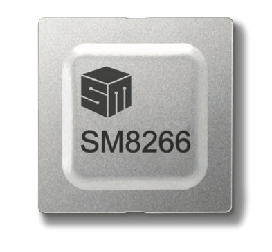
Silicon Motion SM8266 Controller
Silicon Motion's new enterprise NVMe controller is the SM8266, a 16-channel design with a PCIe 4 x4 host interface.
Silicon Motion's first enterprise NVMe controller was the SM2270. That had a bit of an odd design: it essentially combined two 8-channel controllers onto one chip behind a shared PCIe front-end supporting PCIe 3 x8. This allowed Silicon Motion to re-use a lot of the design of their very successful 8-channel client/consumer NVMe controllers while easily scaling up to a 16-channel solution. Silicon Motion hasn't shared a block diagram for the new SM8266, but we suspect they're still using a similar split design since the SM8266 spec sheet mentions dual 32-bit DRAM interfaces.
The SM8266 uses the same 21mmx21mm package as the SM2270 but drops support for an x8 host interface—PCIe 4 x4 is plenty fast. The NAND interface now supports speeds up to 1200MT/s, the same as their recently-released SM2267 mainstream consumer NVMe controller, but a step behind the 1600MT/s supported by their upcoming SM2264 high-end consumer NVMe controller (both 8-channel designs). The DRAM interface on the SM8266 supports DDR4 and LPDDR3 at faster speeds than the SM2270, but again is lagging behind their latest consumer NVMe controllers that support LPDDR4(X).
The SM8266 supports up to 128 IO queues and optional NVMe features like Controller Memory Buffer (CMB) and up to 32 namespaces. Additionally, Silicon Motion can provide firmware implementing an Open Channel SSD interface or Key-Value SSD interface. Open Channel support was a major highlight of the SM2270, which was developed primarily for Alibaba's use. However, most industry interest in Open Channel SSDs has moved on to the newer NVMe Zoned Namespaces standard.
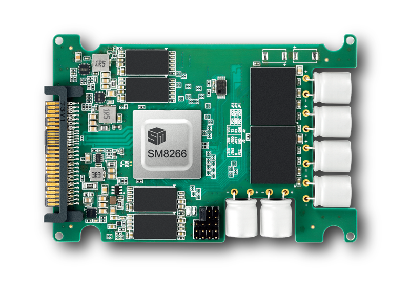
The Silicon Motion SM8266 is available as a turnkey solution of the controller and firmware with SSD hardware reference designs. Silicon Motion's subsidiary Shannon Systems is using the SM8266 in drives for hyperscale customers, expected to go into production in 2021.
| Silicon Motion Enterprise/Datacenter NVMe SSD Controllers | ||||||
| SM8266 | SM2270 | |||||
| DRAM Support | 2x 32bit DDR4-2400, LPDDR3-2133 | 2x 32bit DDR4-2133, LPDDR3-1600 | ||||
| Host Interface | PCIe 4 x4 | PCIe 3 x8 | ||||
| NAND Channels, Interface Speed | 16ch, 1200 MT/s |
16ch | ||||
| CEs per Channel | 8 | 8 | ||||
| Sequential Read | 6550 MB/s | 3200 MB/s | ||||
| Sequential Write | 3100 MB/s | 2800 MB/s | ||||
| 4KB Random Read IOPS | 950k | 800k | ||||
| 4KB Random Write IOPS | 220k | 200k | ||||
Phison FX Series SSDs
The new Phison FX is a bit different from their previous enterprise/datacenter solutions, which have been -DC variants of their client/consumer SSD controllers. The Phison FX Series is a family of SSD reference designs, using a new controller that has not been separately named. The FX Series SSDs are U.2 15mm drives using 96L 3D TLC, with firmware that can be customized to suit the features required by each customer. The FX's controller is a 12-channel design—the widest Phison has ever put out—but the host interface is still just PCIe 3 x4. Despite the older PCIe gen3 host interface, the Phison FX uses their fourth-generation LDPC engine, the same as used in their E16 PCIe gen4 consumer SSD controller. Overall, it's a clear step up from their 8-channel E12DC controller solution, but this is definitely the most conservative of the three new controller designs. However, that also means it is quick to market: Phison has already started shipping these drives.
| Phison Enterprise/Datacenter NVMe SSD Solutions | ||||||
| FX Series | E12DC | |||||
| Host Interface | PCIe 3 x4 | PCIe 3 x4 | ||||
| NAND Channels | 12 | 8 | ||||
| Sequential Read | 3400 MB/s | 3200 MB/s | ||||
| Sequential Write | 2500 MB/s | 1000 MB/s | ||||
| 4KB Random Read IOPS | 560k | 460k | ||||
| 4KB Random Write IOPS | 90k | 70k | ||||
| Performance based on 3.84TB 1 DWPD models | ||||||
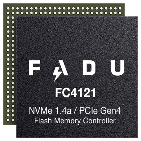
FADU Delta SSDs with FC4121 Controller
FADU is a fairly new SSD controller design firm, having been founded in 2015 and launched their first controller ASIC (FC3081) in 2018. This year, they are launching their second controller, the FC4121. The new controller moves to PCIe 4.0, widens the flash interface from 8 to 12 channels and increases the supported speeds from 800MT/s to 1200MT/s—which means the FC4121 can use almost all the extra bandwidth offered by the faster PCIe host interface.
| FADU Enterprise/Datacenter NVMe SSD Controllers | ||||||
| FC4121 | FC3081 Annapurna |
|||||
| DRAM Support | 32bit DDR4, LPDDR4(X) | 32bit DDR4, LPDDR4 | ||||
| Host Interface | PCIe 4 x4 | PCIe 3 x4 | ||||
| NAND Channels, Interface Speed | 12ch, 1200MT/s |
8ch, 800MT/s |
||||
| CEs per Channel | 16 | 8 | ||||
| Sequential Read | 7.1 GB/s | 3.5 GB/s | ||||
| Sequential Write | 5.1 GB/s | 2.65 GB/s | ||||
| 4KB Random Read IOPS | 1675k | 820k | ||||
| 4KB Random Write IOPS | 450k | 230k | ||||
| Performance based on 28% OP 3 DWPD using SK hynix 128L TLC | ||||||
FADU's SSD controller architecture was the first to use RISC-V processor cores, with their previous FC3081 "Annapurna" controller featuring SiFive's S51 cores. The controller architecture also features a variety of special-purpose hardware offloads to improve power efficiency and QoS. FADU's firmware can support a wide range of the more advanced optional NVMe features, including Controller Memory Buffer (CMB), Persistent Memory Region (PMR), SR-IOV virtualization, IO Determinism and Zoned Namespaces.
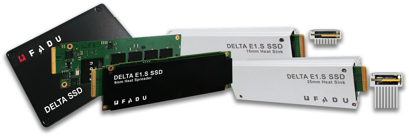
FADU provides their DELTA reference SSD designs based around the FC4121 controller, with both U.2 and EDSFF E1.S designs and firmware customization available. These designs are available either for customers to manufacture themselves, or customers can provide the NAND and FADU will arrange contract manufacturing of the private label SSDs.


5 Comments
View All Comments
croc - Wednesday, November 25, 2020 - link
Why is write speed always the hard part? Whether DC or consumer, it always seems to lag read by a good margin. Seriously, curious about this.Kristian Vättö - Thursday, November 26, 2020 - link
It's down to the fundamental operation of NAND. Read is done by sensing the voltage level, whereas in writes electrons have to be injected to the cell to create the charge. Writes get even harder in multi-level cell variants since the programming has to be done in multiple iterations. For modern TLC, write latency is ~10x higher than read.Calin - Thursday, November 26, 2020 - link
Furthermore, reading is "painless" - i.e. you read the data.Writing in a current SSD (i.e. one based on either MLC or TLC, or even QLC) means you write quickly into flash as "SLC" (i.e. just one bit per cell), and mark the sector to be moved into MLC/TLC/QLC later (MLC = 2 bits per cell, TLC = three bits per cell)
(current consumer SSD are basically TLC with SLC cache).
So, an SSD will have a maintenance process running in the background - hopefully when no other operations are done, but you could swamp the SLC cache and start it.
Furthermore, if flash block A was written into much more often than flash block B, then the contents and addresses of flash block A and flash block B will be swapped (so hopefully the next, often, future drives into block A will in fact use the reliability of block B).
Of course, enterprise level SSDs might have a RAM cache and "battery" - so writes will be initially received at the speed they can be written into the RAM cache (i.e. basically instant as long as the RAM cache has not filled up). The battery is there to give enough energy to write the RAM cache into the flash.
diediealldie - Friday, November 27, 2020 - link
For a NAND, sensing existing election(1 is erased, 0 is written) is quite easy, but moving elections back and forth is quite hard.Funny thing is that in real world, read latency(not throughput!) matters more than write latency. Because small writes can be hidden by DRAM write-back cache, while there is no way to hide read latency from device perspective.
TheinsanegamerN - Monday, November 30, 2020 - link
Others have already answered well. I wanted to add that the way you use datacenter drives is typically over a network interface.For the slowest read speed listed here, the sequential speed would saturate two 10 gigabit network interfaces. The fastest, the FADU, could consume 41Gbps. Most datacenters will usually top out at 4x10Gbps for a BIG data unit. At these speeds most servers will be network bound befor ebeing drive bound, and that's not counting, say, RAID 5 or 6 or custom solutions. DCs faster then this will typically be using PCIe slot based SSDs or optane style devices with much higher read/write speeds and prices to match.