Intel Pentium 4 1.8GHz: One step closer
by Anand Lal Shimpi on July 2, 2001 4:12 AM EST- Posted in
- CPUs
Introducing 4-Layer Pentium 4 Motherboards
If you’ve ever read any of our Motherboard Reviews you’ll know that one determinant of manufacturing cost when making a motherboard is the number of layers that the PCB is made out of. When we mention layers we are talking about the number of physical layers that traces can be routed through in and on the PCB. Think of each layer as a separate plane where traces can be routed independently of another layer (plane); traces can also be connected from one layer to another. The more complex a motherboard layout happens to be, the greater the necessity for having multiple board layers partially to provide greater electrical noise insulation.
Remembering back to one of the original claims Rambus made about RDRAM, a major benefit of the 16-bit serialized RDRAM interface is that it requires fewer traces than 64-bit SDRAM/DDR SDRAM. The argument Rambus made was that with fewer traces, boards could be made on 4-layer designs instead of 6-layer designs. The reality is that until recently every single Pentium 4 motherboard was built on a 6-layer PCB.
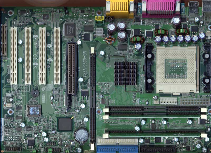
We are finally seeing some 4-layer Pentium 4 motherboards, such as MSI’s 850
Pro2 which we used for this review. If you’ll notice, the most peculiar thing
about the motherboard is that there is one RDRAM slot perpendicular to the other
three. This type of a layout is possible because of the serialized nature of
RDRAM and it is done presumably to save space. These 4-layer boards should
become increasingly more common as we saw a few at this year’s Computex in
Overclocking
One of the benefits of getting your hands on an Intel Engineering Sample CPU is that they come from the factory without any multiplier lock; it makes testing much easier but it also allows you to experiment with higher frequencies to see how stable Intel’s current yields will be when overclocked. Unfortunately, the 18x clock multiplier of our ES Pentium 4 1.8GHz processor (18 x 100MHz = 1800MHz) was the highest multiplier the CPU would accept. Anything higher would default to 18X, although lower multipliers worked just fine.
With the CPU running so cool at 1.8GHz and with Intel scheduled to be at higher than 2GHz before the end of the year, we figured that hitting the big 2.0 mark was worth an effort. So instead of relying on the clock multiplier alone we dropped that down to 15x and increased the FSB frequency from 100MHz to 133MHz. Before you get too confused there remember that the Pentium 4’s FSB is “quad-pumped” meaning that data is sent at 4 times the FSB clock (effectively 400MHz) while addresses are still sent at 1x the FSB clock (100MHz). This is much like AMD’s DDR EV6 bus where data is sent at 2x the FSB clock (effectively 200/266MHz) while addresses again are only sent once per clock.
This overclock worked flawlessly and we managed to run the CPU at 2.0GHz (15 x 133MHz) at 1.70V without any additional cooling. In order to make the system stable at this frequency we had to decrease the RDRAM multiplier from 4X down to 3X which actually kept our RDRAM in spec at PC800 (4 x 100MHz = 400MHz = 3 x 133MHz). The Pentium 4 FSB was effectively clocked at 533MHz which resulted in a bit of the increased performance that we noticed from our overclocked setup.
Newer Pentium 4 1.5GHz processors may have similar successes since they also use the 15x multiplier. If you happen to have a 1.5GHz Pentium 4, try your hand at overclocking it to 133MHz x 15 (be sure to turn down your RDRAM multiplier/frequency) and post your results to our CPU Database.


0 Comments
View All Comments