Analyzing Intel-Micron 3D XPoint: The Next Generation Non-Volatile Memory
by Kristian Vättö, Ian Cutress & Ryan Smith on July 31, 2015 11:00 AM EST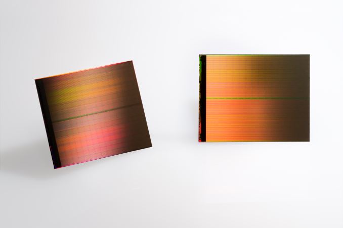
The current mainstream memory technologies, namely DRAM (quick memory accessed by the processor) and NAND (solid-state storage), have been around for decades. While the cell designs have evolved over the years to allow scaling to 20nm and below, the fundamental physics behind DRAM and NAND operation haven't changed a bit and both technologies have their unique technological limitations. DRAM offers nanosecond-level latency and unlimited endurance, but this comes at the cost of large cell size, cell volatility, and power consumption. Since DRAM cells need to be constantly refreshed, the cells don't retain data in an off state, requiring quite a bit of power and making DRAM unsuitable for permanent storage. NAND, on the other hand, has much higher latency (especially write operations) and has a limited number of write cycles, but the cells are non-volatile and the structure is much more efficient, enabling low cost and suitability for storage.
Combining DRAM and NAND at the system-level architecture provides the best of both worlds, which is why modern computers use DRAM as a memory/cache and NAND for storage. However, there's still a latency and capacity gap between DRAM and NAND, so the question arises: what if you were to combine the best of DRAM and NAND at the silicon level? The mission of next generation memory technology across the industry has been to develop a new type of memory that provides low latency and high endurance while offering a small and scalable cell size.
We have seen numerous startups, such as Crossbar and Nantero, discuss and demonstrate their next generation memory technologies, but we have yet to see the established DRAM and NAND vendors come out with their solutions. Intel and Micron are here to change that with the announcement of their new 3D XPoint (Cross Point) non-volatile memory technology this week.
First and foremost, Intel and Micron are making it clear that they are not positioning 3D XPoint as a replacement technology for either NAND or DRAM, and in that scale it has been talked about more in its applications nearer NAND than DRAM. It's supposed to complement both and provide a technology that sits in between the two by filling the latency and cost gap exists between DRAM and NAND. Basically, 3D XPoint is a new tier in the computer architecture because it can be used as either slower, non-volitile memory or much faster storage.
| DRAM | 3D XPoint | NAND | |
| Endurance (P/E Cycles) | 10^15 | 10^7 | 10^3 |
| Read Latency | Nanoseconds | 10s of Nanoseconds | ~100 Microseconds |
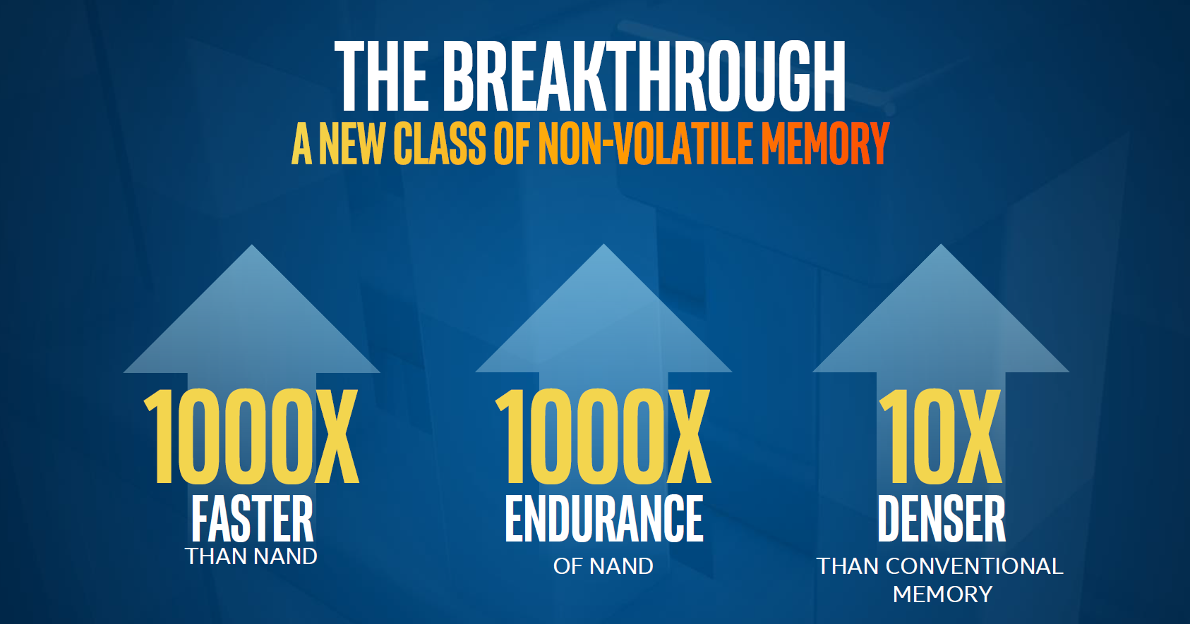
Intel and Micron are claiming that 3D XPoint provides up to a thousand times higher endurance than NAND. Assuming that the numbers are relative to modern (15-20nm) MLC NAND, the endurance should be in the order of a few million P/E cycles; though the marketing materials are claiming up to tens of millions of write cycles. If we assume 3 million write cycles (1000x of what modern MLC has), a 256GB 3D XPoint based drive would have a total write endurance of 768 petabytes. That's equivalent to 420TB per day for five years, or 4.9GB per second. For storage applications that currently rely on NAND, 3D XPoint will eliminate any potential endurance concerns, but it's not durable enough to challenge DRAM in that front since DRAM endurance is essentially infinite. Whether 3D XPoint provides enough endurance to replace DRAM ultimately depends on the application, but especially in certain enterprise workloads there's a need for DRAM.
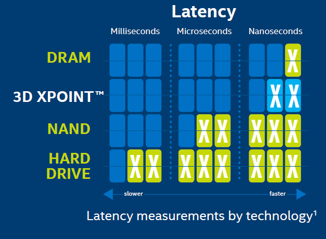
3D XPoint latency should be in the order of 10s of nanoseconds, but the companies didn't specify whether this is read or write latency. Judging by the graphs provided by Intel, it seems to be read latency because NAND write latency would measured in milliseconds (typically 1-2ms for a full page write), whereas the graph puts NAND latency at tens of microseconds that is in line with NAND read latency. Write latency is likely higher than that, probably at least 100s of nanoseconds or even a few microseconds given Intel and Micron's claims of "up to 1000x faster than NAND", but what complicates things is that 3D XPoint is accessible at the bit-level whereas NAND is page-level, so comparing the latency of the two without extended context is quite difficult. In any case, 3D XPoint performance should be closer to DRAM than NAND, but since Intel and Micron aren't discussing any specific latencies yet it's too early to make any final conclusions.
Meanwhile unlike many next generation memory technologies out there at the moment, 3D XPoint is the furthest along and doesn't only exist on paper or in a lab. Intel and Micron are currently sampling the first generation die that is being produced at the companies' jointly owned fab in Lehi, Utah. The die is 128Gbit (16GB) in capacity, whereas the products that startup memory companies have in production are in the order of dozens of megabytes. The die is built on a 20nm node and consists of two layers, and in the future scaling will happen through both lithography shrinks and by increasing the number of layers.
The Utah fab has been producing 20nm NAND for now since Intel didn't invest on the 16nm shrink and all initial 3D NAND production will take place in Micron's Singapore fab, but it's unclear whether the full fab with its 20,000 wafers per month capacity will be dedicated to 3D XPoint from now on. My guess would be that 3D XPoint will gradually take over the full wafer capacity in Utah depending on how the market reacts to the new technology and how high demand Intel and Micron are seeing. 3D XPoint does require some new equipment for manufacturing since 3D XPoint deals with a whole new set of materials, but Intel and Micron said that the transition is quite similar to a new NAND node and allows some of the existing equipment to be used.
The companies aren't quoting any price per gigabyte yet, but since the whole function of 3D XPoint is to fill the gap between DRAM and NAND, it will also be priced accordingly. A quick look at NewEgg puts DRAM pricing at approximately $5-6 per gigabyte, whereas the high-end enterprise SSDs are in the range of $2-3. While client SSDs can be had for as low as $0.35, they aren't really a fair comparison because at least initially 3D XPoint will be aimed for enterprise applications. My educated guess is that the first 3D XPoint based products will be priced at about $4 per gigabyte, possibly even slightly lower depending on how DRAM and NAND pricess fall within a year.


80 Comments
View All Comments
Pork@III - Friday, July 31, 2015 - link
1000X1000X10=3 Touch my crazy math! "Analyze This"Wwhat - Saturday, August 8, 2015 - link
Didn't intel slides on future CPU's talk about the new RAM? That would mean they might create their own market and there is no need to hope someone is interested really, if it's architecturally a (semi-)requirement for intel based systems.Wwhat - Saturday, August 8, 2015 - link
Oh excuse me, wasn't meant to be a reply but a standalone comment.Russ.Dill@gmail.com - Friday, July 31, 2015 - link
I was really excited about this article due to the leadup on Twitter. But I'm really disappointed on the coverage of the technology.I think Ian has a bit of confirmation bias going into this and did not examine PCM closely enough:
> During the discussions after the announcement, we were told
> categorically that this is not a phase change material, eliminating
> one potential avenue that it might be the change in the crystal
> structure of the cell producing the resistance change.
Here's the portion of the webcast:
https://www.youtube.com/watch?v=VsioS35D-HY&t=...
"So…so let me take the first piece while Rob you jump in. First…first of all you shouldn't think of this as NAND or DRAM. You should think of it as a whole new class of memory. It…it…it…it really does fill it's own unique spot. Now it can be used in more of a storage type of application or it can be used more as a system main memory and we think it will be used as both. Uh…uh f…for different applications and different reasons. Um, but it really kinda fits in that…in that unique spot.
Now rel…I'm not familiar with sigma RAM I'm sorry maybe…maybe Rob is, but…but relative to…to phase change which has been the market before and which Micron has some experience with in the past. Uh, again, this is uh, this is a, this is a…a very different architecture in terms of the place it fills in the…in the…in the memory hierarchy because it has these…these dramatic improvements, uh, in speed, uh, and…and volatility and, uh, performance."
I don't view that as a categorical denial that it's PCM. Just that it's a different architecture than the PCM product had out before, which it is. This is cross point. And there is a lot of hesitation in this response and it seems like rather than trying to answer the technology question, he goes back on message.
Along with patents, linkedin profiles (Employee confirms working on a 2xnm PCM 3D cross-point chip since January 2014, see Giulio Albini), and the mentions in the webcast of "property change" and "bulk material".
Russ.Dill@gmail.com - Friday, July 31, 2015 - link
The interesting thing is that 2xnm PCM cross point technology has been on the roadmap for a while, but in 2014, mention of PCM was phased out. The 2014/2015 materials still mention "other technologies" though. It could be that the technology failed. It seems more likely that there is some legal or corporate strategy for not mentioning the technology.2013 Fall and Summer slides: http://i.imgur.com/pAHeUPH.png
Ian Cutress - Friday, July 31, 2015 - link
We had a separate question and answer session with Greg Matson, SSD Director at Intel. When specifically asked if it was PCM, he said he could confirm that it was not.Russ.Dill@gmail.com - Friday, July 31, 2015 - link
I'm guessing this Q/A session was not recorded, can you give an actual quote? Are they just arguing semantics and claiming that it is PCMS?Ian Cutress - Friday, July 31, 2015 - link
OK now that I'm at a computer I can respond properly.Kristian attended the event live, I was at the UK briefing led by Greg Matson, so all questions on my end went through him with other press based in the UK, so no it was not recorded. It was specifically asked 'Is this Phase Change?' and he responded 'I can confirm it is not Phase Change'. The other journalist at that Q&A that I've seen pick up on this was the one that asked the question, Chris Mellor from The Register. Check his tweets on the subject as a double confirmation:
https://twitter.com/Chris_Mellor/status/6267342455...
https://twitter.com/Chris_Mellor/status/6267347543...
If you read through Chris' piece on XPoint, he comes to similar conclusions based that a 64Mb phase change demo with an ovonic switch last year was different to Micron's slide demonstration of XPoint with a diode-based selector.
So standard PCM/PCMS revolves around bulk crystal structure changes and metastable forms to differentiate resistive states, hence the 'phase' part of phase change. Arguably conductive bridging is also a change in phase, from a charged ion to a conducting metal, although is not specifically called phase change as such. It could also not necessarily be called a 'bulk change' as mentioned by Intel, although if the electrolyte layer is thin it would certainly act like bulk between the electrodes.
PCM, as of last year, was also considered one of the front runners leading into the technology based on information released although there have been reservations based on the currentneeded to transition current materials and the respective heat. Given Micron's investor briefing slides, conductive bridging is still perhaps the most likely, especially given how Matson answered the PCM question with an affirmative no. I understand that a few analysts have stated is PCM, given the watchful eye on patents and so forth, but coming direct from the source is hard to ignore with all the other suggestions.
As Kristian points out, Micron's investor roadmap points to a second technology in a couple of years also entering the market. If this isn't PCM, that could be, or vice versa. Or even STT.
Just for the record I'm merely trying to pinpoint where the evidence leads me, rather than introduce any sort of bias here. Without a direct SEM or quote from Intel, we can't be sure. Both PCM and CB can be done with many different materials, and I'd hazard a guess there are combinations that haven't been made public. So we're still talking about general methodology rather than specific physical interations between named structures.
If anyone comes up with anything else, I'd be glad to hear and read it.
Russ.Dill@gmail.com - Friday, July 31, 2015 - link
They have two future memory tech on their timeline, A and B. Perhaps we are seeing A now, and B is phase change.Russ.Dill@gmail.com - Friday, July 31, 2015 - link
BTW, I am still leaning very strongly towards PCM. It of course seems unlikely in the highest degree that Matson could of misspoken on something so basic. Maybe I'm not familiar enough with the tech industry, but it seems so very strange that they are so cagey on the tech. There must be a very strongly company wide memo from legal. They seem to be able to confirm that it is a resistive memory element, but nothing beyond that. So from that aspect, it seems strange that someone would be willing to go on record stating what type of resistive memory element it is not.Given the number of companies with promising cross point style resistive memory architectures (many of them PCM, eg, ST), and the patent warchests to go with them, there is likely to be a legal battle that will make the whole RAMBUS thing seem like it was a small claims case.
I wonder what event is gating release of tech details. Is it a legal agreement? A patent date? A pending legal action?